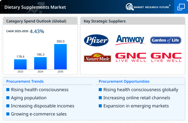
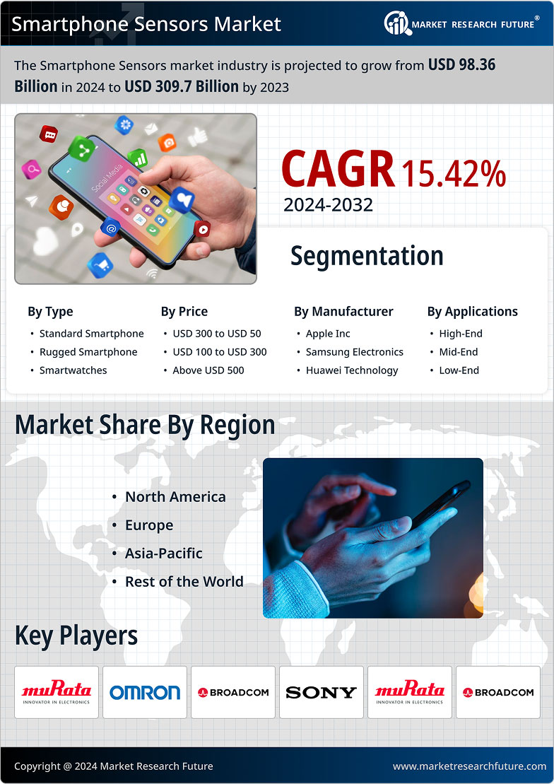
• Cat-intel
  • MedIntelliX
  • Resources
  • About Us
  • English
    Chinese
    French
    Hindi

    3D Semiconductor Packaging Market

    ID: 6279
    113 Pages
    Research Team
    04/2019

    3D Semiconductor Packaging Market Research Report Information By Technology (3D Through Silicon Via, 3D Package on Package, 3D Fan Out Based and 3D Wire Bonded), By End User (Telecommunication, Consumer Electronics, Industrial, and Others) And By Region (North America, Europe, Asia-Pacific, And The Rest Of The World) –Market Forecast Till 2032

    Share:
    ReportInfographic
    $ 4,950.0
    $ 5,950.0
    $ 7,250.0

    Market Summary

    Global 3D Semiconductor Packaging Market Overview:

    3D Semiconductor Packaging Market Size valued at USD 12.2 Billion in 2023. The 3D Semiconductor Packaging market industry is projected to grow from USD 14.1825 Billion in 2024 to USD 40.7 Billion by 2032, exhibiting a compound annual growth rate (CAGR) of 14.09% during the forecast period (2024 - 2032). Increased demand for the miniaturization of electric devices and fast growth in information and communications industries are the key market drivers enhancing the growth of market.

    3D Semiconductor Packaging Market Overview

    Source: The Secondary Research, Primary Research, MRFR Database, and Analyst Review

    3D Semiconductor Packaging Market Trends

      • Growing demand for miniaturization in electric devices is driving the market growth.

    Market CAGR for 3D semiconductor packaging is being driven by the rising demand for miniaturization in electric devices. The rising demand for devices with high capacity and less storage is expected to increase the demand for 3D semiconductor packaging. The tendency towards miniaturization is becoming important in the creation and design of electronic devices. The method provides important advantages like heterogeneous integration, in which the circuit layers are designed using different processes on different wafers.

    Microelectronic devices consist of small surgical apparatus used in the healthcare industry and miniature MEMS devices employed in electronic products and others. These devices consist of different integrated chips, in which the producers emphasize their size minimization. Low power and small-size consumption are the main factors driving the demand for chips with several advanced semiconductor packaging techniques, from which one is 3D packaging design. The demand for the compact electronic circuit is boosted with the reduced size of electronic devices for ease of access for customers. The increasing technological superiorities over 2D packaging technology, increase in requirement for miniaturized circuits in microelectronic devices, growing demand for tablets, wearable devices, low-end smartphones, and other connected consumer goods, rising demand for consumer electronic products, increasing sales of MEMS devices, enhanced efficiency, and less power consumption are main factors boosting the growth of 3D semiconductor packaging market.

    Compared to traditional wired technologies, 3D integrated circuit wires have a huge capacitance. Sensitive circuits are further separated into different levels to conceal the purpose of each layer. Greater chip connectivity compared to conventional layouts is another goal of 3D IC technology. Products currently are getting smaller while incorporating greater utility. It is typical for the miniaturization of one stage of a product to disclose constraints and challenges in the entire design and production process.

    The latest advancement in technologies has new gadgets coming up in the market, like e-book readers, tablet computers, gaming devices, 3D smart glass, and virtual reality products that demand s high-performance electronic components. The market expansion is expected to be boosted by the increase in demand for compact electronic devices in end-user sections like healthcare, consumer electronics, and automotive. The key market participants are focusing on making electrical goods smaller, which is one of the essential components of contemporary consumer goods. Tiny gadgets are utilized in the technology industries and medicine. Thus, driving the 3D Semiconductor Packaging market revenue.

    3D Semiconductor Packaging Market Segment Insights:

    3D Semiconductor Packaging Technology Insights

    The 3D Semiconductor Packaging Market segmentation, based on technology, includes 3D Through Silicon Via, 3D Package on Package, 3D Fan Out Based, and 3D Wire Bonded. The 3D through silicon via segment dominates the market, accounting for the largest market revenue due to the rising demand for TSV-based packages owing to their superior performance features like high-speed data transfer and low power consumption compared to traditional 2D packages.

    3D Semiconductor Packaging End User Insights

    The 3D Semiconductor Packaging Market segmentation, based on end users, includes Telecommunication, Consumer Electronics, Industrial, and Others. The consumer electronics segment dominates the market owing to the growing use of 3D semiconductors in flat panel television sets, personal computers, and other home appliances. The rapid development of smart devices is expected to boost growth of market during the forecast years. 3D semiconductor packaging can be utilized in several industrial applications, including aerospace, electronic devices, defense equipment, medical systems and devices, and consumer electronics. The 3D semiconductor packaging prevents devices from being damaged by exterior forces and offers a more efficient and secure way of packing components, and minimizes the heat fluxes within electronic modules, leading to enhanced performance and stability.

    Figure 1: 3D Semiconductor Packaging Market by End User, 2022 & 2032 (USD Billion)

    3D Semiconductor Packaging Market by End User, 2022 & 2032

    Source: The Secondary Research, Primary Research, MRFR Database and Analyst Review

    3D Semiconductor Packaging Regional Insights

    By region, the study offers market insights into North America, Europe, Asia-Pacific, and the Rest of the World. The North American 3D Semiconductor Packaging market area, dominates the market due to the strong growth of the electronics industry and the preference for miniaturized electronic devices that are compact and don't compromise on power. Further, the fast adoption of high-end electronic devices and the growth of machine learning and AI technologies in this region is anticipated to boost the growth of the market.

    Further, the prime countries studied in the market report are the US, Canada, German, France, the UK, Italy, Spain, Japan, India, China, Australia, South Korea, and Brazil.

    Figure 2: 3D Semiconductor Packaging Market SHARE BY REGION 2022 (USD Billion)

    3D Semiconductor Packaging Market SHARE BY REGION 2022

    Source: The Secondary Research, Primary Research, MRFR Database, and Analyst Review

    The Asia-Pacific 3D Semiconductor Packaging Market accounts for the second-largest market revenue due to the rising production of semiconductors and large range usage of 3D semiconductor packaging, and the presence of key market players in this region. Moreover, China’s 3D Semiconductor Packaging market held the largest market share, and the Indian 3D Semiconductor Packaging market was the rapid-growing market in the Asia-Pacific region.

    Europe's 3D Semiconductor Packaging market is expected to grow at the fastest CAGR from 2023 to 2032. This is due to the rising adoption of 3D semiconductor packaging in this region. Further, the German 3D Semiconductor Packaging market held the largest market share, and the UK 3D Semiconductor Packaging market was the fastest-growing market in the European region.

    3D Semiconductor Packaging Key Market Players & Competitive Insights

    Leading market players are investing heavily in research and development in order to expand their product lines, which will help the 3D Semiconductor Packaging market grow even more. Market players are also undertaking various strategic activities to expand their global footprint, with important market developments including new product launches, contractual agreements, mergers and acquisitions, higher investments, and collaboration with other organizations. To expand and survive in a more competitive and rising market climate, the 3D Semiconductor Packaging industry must offer cost-effective items.

    Manufacturing locally to minimize operational costs is one of the key business tactics used by manufacturers in the global 3D Semiconductor Packaging industry to benefit clients and increase the market sector. In recent years, the 3D Semiconductor Packaging industry has offered some of the most significant advantages to electronic industries. Major players in the 3D Semiconductor Packaging market, including Samsung Electronics Co Ltd., United Microelectronics Corporation, Intel Corporation, ACM Research, Taiwan Semiconductor Manufacturing Company, ASE Technology Holdings Co. Ltd., Amkor Technology, Jiangsu Changjiang Electronics Technology Co. Ltd., and others, are attempting to increase market demand by investing in research and development operations.

    Samsung Electronics, founded on March 1938, is a South Korean company, one of the world's largest producers of electronic devices. The company specializes in the production of a large variety of consumer and industry electronics, including appliances, semiconductors, digital media devices, integrated systems, and memory chips. The company has become one of the most recognizable brands in technology and manufactures about a fifth of South Korea's total exports. In July 2022, Samsung Electronics Co. initiated its mass manufacturing of 3-nanometer semiconductor chips for a Chinese cryptocurrency miner. These chips are expected to minimize power consumption by 50% and enhance performance by 30%, as stated by Samsung Electronics Co.

    United Microelectronics Corporation, a Taiwanese company based in Hsinchu, Taiwan, is a leading global semiconductor foundry company, providing high-quality IC fabrication services, emphasizing logic different specialty technologies to serve all main sectors of the electronics industry. The company designs produces, and markets ICs and related electronic products. The main products of the company are consumer electronics ICs, personal computer peripheral ICs, memory ICs, and communication ICs. In February 2023, the company and Cadence collaborated on 3D-IC Hybrid Bonding Reference Flow. This technology helps the integration throughout a large range of technology nodes suitable for edge AI, wireless communication applications, and image processing. The design reliability and cost-effectiveness are factors of UMC's hybrid bonding technologies, and partnership with Cadence offers mutual customers helping them reap the benefits of 3D structures.

    Key Companies in the 3D Semiconductor Packaging market include

      • Samsung Electronics Co Ltd.

      • United Microelectronics Corporation

      • Intel Corporation

      • ACM Research

      • Taiwan Semiconductor Manufacturing Company

      • ASE Technology Holdings Co. Ltd.

      • Amkor Technology

      • Jiangsu Changjiang Electronics Technology Co. Ltd.

    3D Semiconductor Packaging Industry Developments

    In June 2024, at a press release that showed its unveiling of innovations in producing semiconductor package substrates, the Japanese company and a chemical manufacturer, Shin-Etsu Chemical Co., Ltd., explained their work with micro-LED manufacturers on new technologies and also their equipment for the company.

    In February 2024, it came to light that there are other companies that are working and competing with Intel Corporation, which is primarily engaged in manufacturing and selling microprocessors for computers. Intel confirmed further developments with a foundry strategy targeted towards the AI Age. By 2030, Intel intends to be the second-largest foundry globally. Three other executives that were in attendance were Open AI Sam Altman, Arm CEO Rene Hass production capabilities, and U.S. Secretary Gina Raimondo. A steering roadmap that entails guardians for Intel 3, Intel 18A, and Intel 14A processes has also been shifted.

    In 2023, Intel continued to innovate with the introduction of new packaging systems. They announced a novel form of semiconductor packaging called Foveros Omni which is a three-dimensional stacked configuration packaging technology that allows several dies to be placed one on top of the other in order to greatly enhance the performance level of the power efficiency ratio.

    In November 2022, a Samsung semiconductor project for a wafer-to-wafer to three-dimensional IC was launched with Engro’s Nebula project which was developed in partnership with Advanced Semiconductor Engineering Incorporation as a package company. Other companies that joined in this initiative include Cadence, Faraday Technology and Winbond Electronics. The growth in 3D tools has now been increased by the semiconductor manufacturing company based in Taiwan with W2W technology for their major clients.

    In 2022, ASE Group claimed to have made a substantial breakthrough with the introduction of CoWoS Plus adding to the growing list of advancements within the semiconductor packaging sector. CoWoS Plus is a fan-out wafer-level packaging technology that promises to reduce the number of dies required than that of other available fan-out wafer-level packaging technologies, ultimately improving the cost and performance aspects of the unit.

    July 2022: The production of 3D semiconductor chips was announced by Intel Corporation for Media Tek, a Taiwan chip design firm. The first product will be utilized in smart devices with the assistance of Intel 16 technology. This will help Intel Corporation to fuel its foundry business.

    March 2022: KaraMD announced Pure Health Apple Cider Vinegar Gummies, a vegan gummy aimed to aid ketosis, digestion regulation, weight management, and encourage greater levels of energy.

    3D Semiconductor Packaging Market Segmentation:

    3D Semiconductor Packaging Type Outlook

      • 3D Through Silicon Via

      • 3D Package on Package

      • 3D Fan Out Based

      • 3D Wire Bonded

    3D Semiconductor Packaging End User Outlook

      • Telecommunication

      • Consumer Electronics

      • Industrial

      • Others

    3D Semiconductor Packaging Regional Outlook

      • North America

        • US

        • Canada

      • Europe

        • Germany

        • France

        • UK

        • Italy

        • Spain

        • Rest of Europe

      • Asia-Pacific

        • China

        • Japan

        • India

        • Australia

        • South Korea

        • Australia

        • Rest of Asia-Pacific

      • Rest of the World

        • Middle East

        • Africa

        • Latin America

    Market Size & Forecast

    Report Attribute/Metric Details
    Market Size 2023 USD 12.2 Billion
    Market Size 2024 USD 14.1825 Billion
    Market Size 2032 USD 40.7 Billion
    Compound Annual Growth Rate (CAGR) 14.09% (2024-2032)
    Base Year 2023
    Market Forecast Period 2024-2032
    Historical Data 2018- 2022
    Market Forecast Units Value (USD Billion)
    Report Coverage Revenue Forecast, The Market Competitive Landscape, Growth Factors, and Trends
    Segments Covered Technology, End User, and Region
    Geographies Covered North America, Europe, Asia Pacific, and the Rest of the World
    Countries Covered The US, Canada, German, France, UK, Italy, Spain, Japan, India, China, Australia, South Korea, and Brazil
    Key Companies Profiled Samsung Electronics Co Ltd., United Microelectronics Corporation, Intel Corporation, ACM Research, Taiwan Semiconductor Manufacturing Company, ASE Technology Holdings Co. Ltd., Amkor Technology, Jiangsu Changjiang Electronics Technology Co. Ltd.  
    Key Market Opportunities Increasing utilization of semiconductors in power amplifiers for supporting the growth of the market.
    Key Market Dynamics Increased demand for miniaturization of electric devices.

    Major Players

    3D Semiconductor Packaging Market Segmentation

    3D Semiconductor Packaging Type Outlook (USD Billion, 2018-2032)

    • 3D Through Silicon Via

    • 3D Package on Package

    • 3D Fan Out Based

    • 3D Wire Bonded

    3D Semiconductor Packaging End User Outlook (USD Billion, 2018-2032)

    • Telecommunication

    • Consumer Electronics

    • Industrial

    • Others

    3D Semiconductor Packaging Regional Outlook (USD Billion, 2018-2032)

    • North America Outlook (USD Billion, 2018-2032)

      • North America 3D Semiconductor Packaging by Type

        • 3D Through Silicon Via

        • 3D Package on Package

        • 3D Fan Out Based

        • 3D Wire Bonded

      • North America 3D Semiconductor Packaging by End User

        • Telecommunication

        • Consumer Electronics

        • Industrial

        • Others

      • US Outlook (USD Billion, 2018-2032)

      • US 3D Semiconductor Packaging by Type

        • 3D Through Silicon Via

        • 3D Package on Package

        • 3D Fan Out Based

        • 3D Wire Bonded

      • US 3D Semiconductor Packaging by End User

        • Telecommunication

        • Consumer Electronics

        • Industrial

        • Others

      • CANADA Outlook (USD Billion, 2018-2032)

      • CANADA 3D Semiconductor Packaging by Type

        • 3D Through Silicon Via

        • 3D Package on Package

        • 3D Fan Out Based

        • 3D Wire Bonded

      • CANADA 3D Semiconductor Packaging by End User

        • Telecommunication

        • Consumer Electronics

        • Industrial

        • Others

    • Europe Outlook (USD Billion, 2018-2032)

      • Europe 3D Semiconductor Packaging by Type

        • 3D Through Silicon Via

        • 3D Package on Package

        • 3D Fan Out Based

        • 3D Wire Bonded

      • Europe 3D Semiconductor Packaging by End User

        • Telecommunication

        • Consumer Electronics

        • Industrial

        • Others

      • Germany Outlook (USD Billion, 2018-2032)

      • Germany 3D Semiconductor Packaging by Type

        • 3D Through Silicon Via

        • 3D Package on Package

        • 3D Fan Out Based

        • 3D Wire Bonded

      • Germany 3D Semiconductor Packaging by End User

        • Telecommunication

        • Consumer Electronics

        • Industrial

        • Others

      • France Outlook (USD Billion, 2018-2032)

      • France 3D Semiconductor Packaging by Type

        • 3D Through Silicon Via

        • 3D Package on Package

        • 3D Fan Out Based

        • 3D Wire Bonded

      • France 3D Semiconductor Packaging by End User

        • Telecommunication

        • Consumer Electronics

        • Industrial

        • Others

      • UK Outlook (USD Billion, 2018-2032)

      • UK 3D Semiconductor Packaging by Type

        • 3D Through Silicon Via

        • 3D Package on Package

        • 3D Fan Out Based

        • 3D Wire Bonded

      • UK 3D Semiconductor Packaging by End User

        • Telecommunication

        • Consumer Electronics

        • Industrial

        • Others

      • ITALY Outlook (USD Billion, 2018-2032)

      • ITALY 3D Semiconductor Packaging by Type

        • 3D Through Silicon Via

        • 3D Package on Package

        • 3D Fan Out Based

        • 3D Wire Bonded

      • ITALY 3D Semiconductor Packaging by End User

        • Telecommunication

        • Consumer Electronics

        • Industrial

        • Others

      • SPAIN Outlook (USD Billion, 2018-2032)

      • Spain 3D Semiconductor Packaging by Type

        • 3D Through Silicon Via

        • 3D Package on Package

        • 3D Fan Out Based

        • 3D Wire Bonded

      • Spain 3D Semiconductor Packaging by End User

        • Telecommunication

        • Consumer Electronics

        • Industrial

        • Others

      • Rest Of Europe Outlook (USD Billion, 2018-2032)

      • Rest Of Europe 3D Semiconductor Packaging by Type

        • 3D Through Silicon Via

        • 3D Package on Package

        • 3D Fan Out Based

        • 3D Wire Bonded

      • REST OF EUROPE 3D Semiconductor Packaging by End User

        • Telecommunication

        • Consumer Electronics

        • Industrial

        • Others

      • Asia-Pacific Outlook (USD Billion, 2018-2032)

      • Asia-Pacific 3D Semiconductor Packaging by Type

        • 3D Through Silicon Via

        • 3D Package on Package

        • 3D Fan Out Based

        • 3D Wire Bonded

      • Asia-Pacific 3D Semiconductor Packaging by End User

        • Telecommunication

        • Consumer Electronics

        • Industrial

        • Others

      • China Outlook (USD Billion, 2018-2032)

      • China 3D Semiconductor Packaging by Type

        • 3D Through Silicon Via

        • 3D Package on Package

        • 3D Fan Out Based

        • 3D Wire Bonded

      • China 3D Semiconductor Packaging by End User

        • Telecommunication

        • Consumer Electronics

        • Industrial

        • Others

      • Japan Outlook (USD Billion, 2018-2032)

      • Japan 3D Semiconductor Packaging by Type

        • 3D Through Silicon Via

        • 3D Package on Package

        • 3D Fan Out Based

        • 3D Wire Bonded

      • Japan 3D Semiconductor Packaging by End User

        • Telecommunication

        • Consumer Electronics

        • Industrial

        • Others

      • India Outlook (USD Billion, 2018-2032)

      • India 3D Semiconductor Packaging by Type

        • 3D Through Silicon Via

        • 3D Package on Package

        • 3D Fan Out Based

        • 3D Wire Bonded

      • India 3D Semiconductor Packaging by End User

        • Telecommunication

        • Consumer Electronics

        • Industrial

        • Others

      • Australia Outlook (USD Billion, 2018-2032)

      • Australia 3D Semiconductor Packaging by Type

        • 3D Through Silicon Via

        • 3D Package on Package

        • 3D Fan Out Based

        • 3D Wire Bonded

      • Australia 3D Semiconductor Packaging by End User

        • Telecommunication

        • Consumer Electronics

        • Industrial

        • Others

      • Rest of Asia-Pacific Outlook (USD Billion, 2018-2032)

      • Rest of Asia-Pacific 3D Semiconductor Packaging by Type

        • 3D Through Silicon Via

        • 3D Package on Package

        • 3D Fan Out Based3D Wire Bonded

      • Rest of Asia-Pacific 3D Semiconductor Packaging by End User

        • Telecommunication

        • Consumer Electronics

        • Industrial

        • Others

      • Rest of the World Outlook (USD Billion, 2018-2032)

      • Rest of the World 3D Semiconductor Packaging by Type

        • 3D Through Silicon Via

        • 3D Package on Package

        • 3D Fan Out Based

        • 3D Wire Bonded

      • Rest of the World 3D Semiconductor Packaging by End User

        • Telecommunication

        • Consumer Electronics

        • Industrial

        • Others

      • Middle East Outlook (USD Billion, 2018-2032)

      • Middle East 3D Semiconductor Packaging by Type

        • 3D Through Silicon Via

        • 3D Package on Package

        • 3D Fan Out Based

        • 3D Wire Bonded

      • Middle East 3D Semiconductor Packaging by End User

        • Telecommunication

        • Consumer Electronics

        • Industrial

        • Others

      • Africa Outlook (USD Billion, 2018-2032)

      • Africa 3D Semiconductor Packaging by Type

        • 3D Through Silicon Via

        • 3D Package on Package

        • 3D Fan Out Based

        • 3D Wire Bonded

      • Africa 3D Semiconductor Packaging by End User

        • Telecommunication

        • Consumer Electronics

        • Industrial

        • Others

      • Latin America Outlook (USD Billion, 2018-2032)

      • Latin America 3D Semiconductor Packaging by Type

        • 3D Through Silicon Via

        • 3D Package on Package

        • 3D Fan Out Based

        • 3D Wire Bonded

      • Latin America 3D Semiconductor Packaging by End User

        • Telecommunication

        • Consumer Electronics

        • Industrial

        • Others

    Market Trends

    Global 3D Semiconductor Packaging Market Overview:

    3D Semiconductor Packaging Market Size valued at USD 12.2 Billion in 2023. The 3D Semiconductor Packaging market industry is projected to grow from USD 14.1825 Billion in 2024 to USD 40.7 Billion by 2032, exhibiting a compound annual growth rate (CAGR) of 14.09% during the forecast period (2024 - 2032). Increased demand for the miniaturization of electric devices and fast growth in information and communications industries are the key market drivers enhancing the growth of market.

    3D Semiconductor Packaging Market Overview

    Source: The Secondary Research, Primary Research, MRFR Database, and Analyst Review

    3D Semiconductor Packaging Market Trends

      • Growing demand for miniaturization in electric devices is driving the market growth.

    Market CAGR for 3D semiconductor packaging is being driven by the rising demand for miniaturization in electric devices. The rising demand for devices with high capacity and less storage is expected to increase the demand for 3D semiconductor packaging. The tendency towards miniaturization is becoming important in the creation and design of electronic devices. The method provides important advantages like heterogeneous integration, in which the circuit layer...

    Market Segment Insights

    Smartphone Sensors Smartphone Type Insights

    The Smartphone Sensors market segmentation, based on smartphone type, includes standard smartphone, rugged smartphone, smartwatches, and other wearable. The standard smartphone segment dominated the market, accounting for the maximum market revenue. A smartphone is a mobile phone with a built-in computer and advanced features, such as web browsing and operating system, which are not associated with its counterpart. The rising mobile internet use, rising disposable income in developing countries, and high ownership of premium design smartphones are a few factors that are anticipated to grow smartphone sales. Smartphones are helped by a mobile operating system that offers advanced computing facilities. A smartphone can also work as a digital media player for uploading photos, videos, and music through a single interface.

    Smartphone Sensors Market, By Device Type Outlook, 2024 & 2035

    Smartphone Sensors Manufacturer Insights

    The Smartphone Sensors market segmentation, based on the manufacturer, includes Apple Inc., Samsung Electronics, Huawei Technology, Xiaomi Inc., Oppo, Sony Corporation, HMD Global, and others. The Apple Inc. segment generated the most revenue due to its superior quality. Apple’s iPhone stands out over all other smartphones in the market. Apple Inc. is the market leader because they use more sensors in their devices to provide unique features. For Instance: Apple’s iPhone 12 uses a lidar for depth sensing, proximity for 3D touch, a gyroscope for compass, GPS, face ID for biometrics, auto-off, a barometer, a magnetometer for compass & GPS, and an ambient light sensor for auto-dimming displays. The better user experience, increased accessibility, and more security these sensors offer consumers to boost the segment‘s growth.

    Smartphone Sensors Application Insights

    The Smartphone Sensors market segmentation, based on the manufacturer, includes Apple Inc., Samsung Electronics, Huawei Technology, Xiaomi Inc., Oppo, Sony Corporation, HMD Global, and others. The Apple Inc. segment generated the most revenue due to its superior quality. Apple’s iPhone stands out over all other smartphones in the market. Apple Inc. is the market leader because they use more sensors in their devices to provide unique features. For Instance: Apple’s iPhone 12 uses a lidar for depth sensing, proximity for 3D touch, a gyroscope for compass, GPS, face ID for biometrics, auto-off, a barometer, a magnetometer for compass & GPS, and an ambient light sensor for auto-dimming displays. The better user experience, increased accessibility, and more security these sensors offer consumers to boost the segment‘s growth.

    Smartphone Sensors Regional Insights

    The Smartphone Sensors market segmentation, based on the manufacturer, includes Apple Inc., Samsung Electronics, Huawei Technology, Xiaomi Inc., Oppo, Sony Corporation, HMD Global, and others. The Apple Inc. segment generated the most revenue due to its superior quality. Apple’s iPhone stands out over all other smartphones in the market. Apple Inc. is the market leader because they use more sensors in their devices to provide unique features. For Instance: Apple’s iPhone 12 uses a lidar for depth sensing, proximity for 3D touch, a gyroscope for compass, GPS, face ID for biometrics, auto-off, a barometer, a magnetometer for compass & GPS, and an ambient light sensor for auto-dimming displays. The better user experience, increased accessibility, and more security these sensors offer consumers to boost the segment‘s growth.

    Smartphone Sensors Market, By Device Type Outlook, 2024 & 2035

    Smartphone Sensors Price Insights

    The Smartphone Sensors market segmentation, based on price, includes USD 300 to USD 500, USD 100 to USD 300, above USD 500, and under USD 100. The USD 300 to USD 500 segment dominated the market revenue in the projected period. Most smartphones sold in medium-end devices have a sensor within this range. For instance: Nubia launched a new flagship Android device powered by the latest Snapdragon 8Gen 2CPU. The OEM has also specified that this gadget, which peculiarly seems to go by the name Z50 even though its processor was the z40 Pro, will compete with the Xiaomi 13 and iQOO11 series with cutting-edge LPDDR5X RAM and storage with the most recent UFS 4.0 spec.

    Get more detailed insights about 3D Semiconductor Packaging Market

    Key Players and Competitive Insights

    Leading market players are investing heavily in research and development to expand their product lines, which will help the Smartphone Sensors market, grow even more. Market participants are also undertaking various strategic activities to expand their footprint, with important market developments including new product launches, contractual agreements, mergers and acquisitions, higher investments, and collaboration with other organizations. To expand and survive in a more competitive and growing market climate, the Smartphone Sensors industry must offer cost-effective items.

    Manufacturing locally to minimize operational costs is one of the key business tactics manufacturers use in the Smartphone Sensors industry to benefit clients and increase the market sector. In recent years, the Smartphone Sensors industry has offered manufacturers some of the most significant advantages. Major players in the Smartphone Sensors market, including MS AG (Austria), Broadcom Inc. (US), DYNA IMAGE Corporation (China), Murata Electronics Oy (Finland), NEXT Biometrics Group ASA (Norway), Omron Corporation (Japan), Samsung Electronics Co. Ltd. (South Korea), Sony Corporation (Japan)., and others, are attempting to increase market demand by investing in research and development operations.

    Samsung is dedicated to abiding by local laws and regulations and enforcing a strict code of conduct for all employees. Samsung adheres to a straightforward business tent: to usage its technology and expertise to develop top-notch goods and services that make a more cultured world. Samsung provides a high importance on its people and technologies to do this. For Instance: In January 2023, Samsung Electronics launched its new MICRO LED, Neo QLED, and Samsung OLED product lines, along with lifestyle products and accessories, before CES® 2023.

    Apple Inc. is a multinational American technology business with its main office in Cupertino, California. According to revenue, Apple will be the top technological business in the world in 2022, with US $ 394.3 billion in sales. According to market capitalization, Apple is the largest corporation in the world as of March 2023. For Instance: In September 2022, the iPhone 14 and iPhone 14 Plus, which come in two sizes, 6.1 and 6.7 inches and include a smart design, camera upgrades, and game-changing new safety measures, were introduced by Apple. The iPhone 14 and iPhone 14 Plus have a powerful camera system that incorporates the primary and front TrueDepth cameras, the Ultra Wide camera for uncommon perspectives, and the photonic engine, an enhanced picture pipeline.

    Key Companies in the Smartphone Sensors market include

    MS AG (Austria)
    MS AG (Austria)
    MS AG (Austria)
    MS AG (Austria)
    MS AG (Austria)
    MS AG (Austria)
    MS AG (Austria)

    Industry Developments

    • September 2022: Comcast and Samsung Electronics announced their partnership to create 5G Radio Access Network (RAN) technologies to enhance 5G connection for Xfinity Mobile and Comcast Business Mobile users in Comcast service zones. Samsung will provide 5G RAN technology, and Comcast will deploy Citizens Broadband Radio Service (CBRS) and 600 MHz spectrum to provide 5G access to consumer and business users in the US.
    • October 2022: Huawei announced the release of the newest antenna solutions, including the Maxwell platform and the X2 antenna series, for the subsequent 5G antenna innovation stage. The new technologies speed up 5G deployment by improving antenna and setup capabilities.

    Market Segmentation

    Smartphone Type Outlook

    • Standard Smartphone
    • Rugged Smartphone
    • Smartwatches
    • Other Wearable

    Price Outlook

    • USD 300 to USD 500
    • USD 100 to USD 300
    • Above USD 500
    • Under USD 100

    Manufacturer Outlook

    • Apple Inc.
    • Samsung Electronics
    • Huawei Technology
    • Xiaomi Inc.
    • Oppo
    • Sony Corporation
    • HMD Global

    Application Outlook

    • High-Level
    • Mid-Level
    • Low-Level

    Manufacturer Outlook

    North America
    • US
    • Canada
    Europe
    • Germany
    • France
    • UK
    • Italy
    • Spain
    • Rest of Europe
    Asia-Pacific
    • China
    • Japan
    • India
    • Italy
    • Australia
    • South Korea
    • Rest of Asia-Pacific
    Rest of the World
    • Middle East
    • Africa
    • Latin America

    Report Scope

    Report Attribute/Metric Details
    Market Size 2023 USD 12.2 Billion
    Market Size 2024 USD 14.1825 Billion
    Market Size 2032 USD 40.7 Billion
    Compound Annual Growth Rate (CAGR) 14.09% (2024-2032)
    Base Year 2023
    Market Forecast Period 2024-2032
    Historical Data 2018- 2022
    Market Forecast Units Value (USD Billion)
    Report Coverage Revenue Forecast, The Market Competitive Landscape, Growth Factors, and Trends
    Segments Covered Technology, End User, and Region
    Geographies Covered North America, Europe, Asia Pacific, and the Rest of the World
    Countries Covered The US, Canada, German, France, UK, Italy, Spain, Japan, India, China, Australia, South Korea, and Brazil
    Key Companies Profiled Samsung Electronics Co Ltd., United Microelectronics Corporation, Intel Corporation, ACM Research, Taiwan Semiconductor Manufacturing Company, ASE Technology Holdings Co. Ltd., Amkor Technology, Jiangsu Changjiang Electronics Technology Co. Ltd.  
    Key Market Opportunities Increasing utilization of semiconductors in power amplifiers for supporting the growth of the market.
    Key Market Dynamics Increased demand for miniaturization of electric devices.

    Market Highlights

    Author

    Aarti Dhapte
    Team Lead - Research

    She holds an experience of about 6+ years in market research and business consulting, working under the spectrum of information communication technology, telecommunications and semiconductor domains. aarti conceptualizes and implements a scalable business strategy and provides strategic leadership to the clients. her expertise lies in market estimation, competitive intelligence, pipeline analysis, customer assessment, etc.

    Leave a Comment

    Latest Comments

    John Doe
    john@example.com

    This is a great article! Really helped me understand the topic better.

    Posted on July 23, 2025, 10:15 AM
    Jane Smith
    jane@domain.com

    Thanks for sharing this. I’ve bookmarked it for later reference.

    Posted on July 22, 2025, 7:45 PM

    FAQs

    What is boosting the demand for 3D semiconductor packing in the market?

    A host of functional advantages of 3D semiconductor packaging compared to the traditional alternatives along with the surging preference for power-efficient solutions is boosting the market demand.

    What are the trends picking up pace in the market?

    Increasing miniaturization in electronics designing and manufacturing is the latest trend market trend.

    Which country is predicted to be the most lucrative in Asia Pacific?

    China is expected to be the most lucrative market in Asia Pacific.

    What are the packaging methods in the market?

    Through Silicon via (TSV), Package on Package, Through Class Via (TGV) and others are the packaging methods in the market.

    Who are the most prominent end-users in the worldwide market?

    The most prominent end-users in the worldwide market are Military and Aerospace, Telecommunication, Consumer Electronics, Automotive, Industrial, and others.

    Which end-user-based segment can bag the top position in the market?

    The consumer electronic segment can bag the top position in the market in the given timeframe.

    1. Market Introduction
      1. Definition 16
      2. Scope Of The Study 16
      3. List Of Assumptions 17
      4. Market Structure
    2. Research Methodology
      1. Research Process 19
      2. Secondary Research
      3. Primary Research 20
      4. Forecast Model 22
    3. Market Dynamics
      1. Introduction 24
      2. Drivers 24
        1. Rising Demand For Miniaturization
        2. Increasing Use In The Automotive Industry
        3. Driver Impact Analysis 25
      3. Restraints 26
        1. Concerns
        2. Restraint Impact Analysis 26
      4. Opportunities
        1. Proliferation Of IoT And Wireless Devices 26
      5. Supply Chain
      6. Porter’s Five Forces Model 28
        1. Threat Of New
        2. Bargaining Power Of Suppliers 29
        3. Threat Of Substitutes
        4. Bargaining Power Of Buyers 29
        5. Intensity Of Rivalry 29
    4. Market Alerts
      1. Market Trends 31
        1. Current Development In 3D
      2. Use Cases 32
        1. 3D Packaging Technology
        2. 3D Heterogenous Integration Technologies To Support
    5. Global 3D Semiconductor Packaging Market,
      1. Overview 35
        1. 3D SIP (System In Package) 36
        2. 3D SIC 36
        3. 3D IC 36
    6. Global 3D Semiconductor
      1. Overview 38
        1. Package On
        2. Through Silicon Via (TSV) 39
        3. Through Glass Via
        4. Others 39
    7. Global 3D Semiconductor Packaging Market, By
      1. Overview 41
        1. Consumer Electronics 42
        2. Telecommunication`
        3. Industrial 42
        4. Automotive 42
        5. Military & Aerospace
    8. 3D Semiconductor Packaging Market, By Region
      1. Introduction 44
      2. North America 45
        1. US 49
        2. Canada 50
        3. Mexico 52
      3. Europe 54
        1. UK 58
        2. Germany 60
        3. France 62
      4. Asia-Pacific 66
        1. China 70
        2. Japan
        3. India 74
        4. South Korea 76
        5. Rest Of Asia-Pacific
      5. Rest Of The World 80
        1. Middle East & Africa 84
    9. Competitive Landscape
      1. Overview 89
    10. Company
      1. Jiangsu Changjiang Electronics Technology Co., Ltd 92
        1. Financial Overview 92
        2. Products/Solution/Services
        3. Key Developments 93
      2. Intel Corporation 94
        1. Financial Overview 94
        2. Products/Solution/Services
        3. Key Developments 95
        4. SWOT Analysis 95
      3. Siliconware Precision Industries Co., Ltd 96
        1. Financial Overview 96
        2. Products/Solution/Services
        3. Key Developments 97
      4. STMicroelectronics NV 98
        1. Company Overviews 98
        2. Financial Overview 98
        3. Products/Solution/Services
        4. Key Developments 99
        5. SWOT Analysis 99
      5. Xilinx Inc. 100
        1. Company Overviews 100
        2. Products/Solution/Services Offered 101
        3. SWOT Analysis 101
        4. Key Strategy 101
      6. Samsung Electronics Corporation Ltd 102
        1. Company Overview 102
        2. Financial Overview 102
        3. Products/Services Offered 103
        4. SWOT Analysis 103
        5. Key Strategy 103
      7. Taiwan Semiconductor Manufacturing Co. Ltd. 104
        1. Company Overview
        2. Financial Overview 104
        3. Products/Services Offered 105
        4. Key Developments 105
        5. SWOT Analysis 105
        6. Key Strategy
      8. Advanced Semiconductor Engineering Inc. 106
        1. Company Overview
        2. Financial Overview 106
        3. Products/Services Offered 107
        4. Key Developments 107
        5. SWOT Analysis 107
        6. Key Strategy
      9. Ams AG 108
        1. Company Overview 108
        2. Financial
        3. Products/Services Offered 109
        4. Key Developments
        5. SWOT Analysis 109
        6. Key Strategy 109
      10. Amkor
        1. Company Overview 110
        2. Financial Overview
        3. Products/Services Offered 111
        4. Key Developments 111
        5. SWOT Analysis 112
        6. Key Strategy 112
    11. List
    12. GLOBAL 3D SEMICONDUCTOR PACKAGING MARKET, BY REGION, 2024-2032 (USD MILLION) 44
    13. ASIA-PACIFIC: 3D SEMICONDUCTOR PACKAGING MARKET, BY PACKAGING METHOD, 2024-2032
    14. REST OF ASIA-PACIFIC: 3D SEMICONDUCTOR PACKAGING MARKET, BY PACKAGING METHOD,
    15. List Of Figures
    16. GLOBAL 3D SEMICONDUCTOR PACKAGING MARKET, BY PACKAGING METHOD, 2024 VS 2032 (USD
    17. VS 2032 (USD MILLION) 41
    18. VS 2032 (USD MILLION) 80

    3D Semiconductor Packaging Market Segmentation

    3D Semiconductor Packaging Type Outlook (USD Billion, 2018-2032)

    • 3D Through Silicon Via
    • 3D Package on Package
    • 3D Fan Out Based
    • 3D Wire Bonded

    3D Semiconductor Packaging End User Outlook (USD Billion, 2018-2032)

    • Telecommunication
    • Consumer Electronics
    • Industrial
    • Others

    3D Semiconductor Packaging Regional Outlook (USD Billion, 2018-2032)

    • North America Outlook (USD Billion, 2018-2032)

      • North America 3D Semiconductor Packaging by Type

        • 3D Through Silicon Via
        • 3D Package on Package
        • 3D Fan Out Based
        • 3D Wire Bonded
      • North America 3D Semiconductor Packaging by End User

        • Telecommunication
        • Consumer Electronics
        • Industrial
        • Others
      • US Outlook (USD Billion, 2018-2032)

      • US 3D Semiconductor Packaging by Type

        • 3D Through Silicon Via
        • 3D Package on Package
        • 3D Fan Out Based
        • 3D Wire Bonded
      • US 3D Semiconductor Packaging by End User

        • Telecommunication
        • Consumer Electronics
        • Industrial
        • Others
      • CANADA Outlook (USD Billion, 2018-2032)

      • CANADA 3D Semiconductor Packaging by Type

        • 3D Through Silicon Via
        • 3D Package on Package
        • 3D Fan Out Based
        • 3D Wire Bonded
      • CANADA 3D Semiconductor Packaging by End User

        • Telecommunication
        • Consumer Electronics
        • Industrial
        • Others
    • Europe Outlook (USD Billion, 2018-2032)

      • Europe 3D Semiconductor Packaging by Type

        • 3D Through Silicon Via
        • 3D Package on Package
        • 3D Fan Out Based
        • 3D Wire Bonded
      • Europe 3D Semiconductor Packaging by End User

        • Telecommunication
        • Consumer Electronics
        • Industrial
        • Others
      • Germany Outlook (USD Billion, 2018-2032)

      • Germany 3D Semiconductor Packaging by Type

        • 3D Through Silicon Via
        • 3D Package on Package
        • 3D Fan Out Based
        • 3D Wire Bonded
      • Germany 3D Semiconductor Packaging by End User

        • Telecommunication
        • Consumer Electronics
        • Industrial
        • Others
      • France Outlook (USD Billion, 2018-2032)

      • France 3D Semiconductor Packaging by Type

        • 3D Through Silicon Via
        • 3D Package on Package
        • 3D Fan Out Based
        • 3D Wire Bonded
      • France 3D Semiconductor Packaging by End User

        • Telecommunication
        • Consumer Electronics
        • Industrial
        • Others
      • UK Outlook (USD Billion, 2018-2032)

      • UK 3D Semiconductor Packaging by Type

        • 3D Through Silicon Via
        • 3D Package on Package
        • 3D Fan Out Based
        • 3D Wire Bonded
      • UK 3D Semiconductor Packaging by End User

        • Telecommunication
        • Consumer Electronics
        • Industrial
        • Others
      • ITALY Outlook (USD Billion, 2018-2032)

      • ITALY 3D Semiconductor Packaging by Type

        • 3D Through Silicon Via
        • 3D Package on Package
        • 3D Fan Out Based
        • 3D Wire Bonded
      • ITALY 3D Semiconductor Packaging by End User

        • Telecommunication
        • Consumer Electronics
        • Industrial
        • Others
      • SPAIN Outlook (USD Billion, 2018-2032)

      • Spain 3D Semiconductor Packaging by Type

        • 3D Through Silicon Via
        • 3D Package on Package
        • 3D Fan Out Based
        • 3D Wire Bonded
      • Spain 3D Semiconductor Packaging by End User

        • Telecommunication
        • Consumer Electronics
        • Industrial
        • Others
      • Rest Of Europe Outlook (USD Billion, 2018-2032)

      • Rest Of Europe 3D Semiconductor Packaging by Type

        • 3D Through Silicon Via
        • 3D Package on Package
        • 3D Fan Out Based
        • 3D Wire Bonded
      • REST OF EUROPE 3D Semiconductor Packaging by End User

        • Telecommunication
        • Consumer Electronics
        • Industrial
        • Others
      • Asia-Pacific Outlook (USD Billion, 2018-2032)

      • Asia-Pacific 3D Semiconductor Packaging by Type

        • 3D Through Silicon Via
        • 3D Package on Package
        • 3D Fan Out Based
        • 3D Wire Bonded
      • Asia-Pacific 3D Semiconductor Packaging by End User

        • Telecommunication
        • Consumer Electronics
        • Industrial
        • Others
      • China Outlook (USD Billion, 2018-2032)

      • China 3D Semiconductor Packaging by Type

        • 3D Through Silicon Via
        • 3D Package on Package
        • 3D Fan Out Based
        • 3D Wire Bonded
      • China 3D Semiconductor Packaging by End User

        • Telecommunication
        • Consumer Electronics
        • Industrial
        • Others
      • Japan Outlook (USD Billion, 2018-2032)

      • Japan 3D Semiconductor Packaging by Type

        • 3D Through Silicon Via
        • 3D Package on Package
        • 3D Fan Out Based
        • 3D Wire Bonded
      • Japan 3D Semiconductor Packaging by End User

        • Telecommunication
        • Consumer Electronics
        • Industrial
        • Others
      • India Outlook (USD Billion, 2018-2032)

      • India 3D Semiconductor Packaging by Type

        • 3D Through Silicon Via
        • 3D Package on Package
        • 3D Fan Out Based
        • 3D Wire Bonded
      • India 3D Semiconductor Packaging by End User

        • Telecommunication
        • Consumer Electronics
        • Industrial
        • Others
      • Australia Outlook (USD Billion, 2018-2032)

      • Australia 3D Semiconductor Packaging by Type

        • 3D Through Silicon Via
        • 3D Package on Package
        • 3D Fan Out Based
        • 3D Wire Bonded
      • Australia 3D Semiconductor Packaging by End User

        • Telecommunication
        • Consumer Electronics
        • Industrial
        • Others
      • Rest of Asia-Pacific Outlook (USD Billion, 2018-2032)

      • Rest of Asia-Pacific 3D Semiconductor Packaging by Type

        • 3D Through Silicon Via
        • 3D Package on Package
        • 3D Fan Out Based3D Wire Bonded
      • Rest of Asia-Pacific 3D Semiconductor Packaging by End User

        • Telecommunication
        • Consumer Electronics
        • Industrial
        • Others
      • Rest of the World Outlook (USD Billion, 2018-2032)

      • Rest of the World 3D Semiconductor Packaging by Type

        • 3D Through Silicon Via
        • 3D Package on Package
        • 3D Fan Out Based
        • 3D Wire Bonded
      • Rest of the World 3D Semiconductor Packaging by End User

        • Telecommunication
        • Consumer Electronics
        • Industrial
        • Others
      • Middle East Outlook (USD Billion, 2018-2032)

      • Middle East 3D Semiconductor Packaging by Type

        • 3D Through Silicon Via
        • 3D Package on Package
        • 3D Fan Out Based
        • 3D Wire Bonded
      • Middle East 3D Semiconductor Packaging by End User

        • Telecommunication
        • Consumer Electronics
        • Industrial
        • Others
      • Africa Outlook (USD Billion, 2018-2032)

      • Africa 3D Semiconductor Packaging by Type

        • 3D Through Silicon Via
        • 3D Package on Package
        • 3D Fan Out Based
        • 3D Wire Bonded
      • Africa 3D Semiconductor Packaging by End User

        • Telecommunication
        • Consumer Electronics
        • Industrial
        • Others
      • Latin America Outlook (USD Billion, 2018-2032)

      • Latin America 3D Semiconductor Packaging by Type

        • 3D Through Silicon Via
        • 3D Package on Package
        • 3D Fan Out Based
        • 3D Wire Bonded
      • Latin America 3D Semiconductor Packaging by End User

        • Telecommunication
        • Consumer Electronics
        • Industrial
        • Others
    Infographic

    Free Sample Request

    Kindly complete the form below to receive a free sample of this Report

    Customer Strories

    “I am very pleased with how market segments have been defined in a relevant way for my purposes (such as "Portable Freezers & refrigerators" and "last-mile"). In general the report is well structured. Thanks very much for your efforts.”

    Jongwon Byun

    Director, Research Operations
    Case Study

    Smartphone Motherboard Parts Manufacturing Research